HomeGlossary

Semiconductor Glossary

408 terms across the whole industry — materials, process, packaging, test, equipment, facilities, design, smart manufacturing and sustainability. Written for someone meeting the word for the first time.

#
2.5D packaging
Packaging & ATMP
Placing several dies side by side on a shared interposer that provides very dense wiring between them, without stacking them vertically.
300 mm
Twelve-inch waferMaterials & Wafers
The dominant wafer size in high-volume manufacturing. A 300 mm wafer has more than twice the usable area of a 200 mm wafer, which is why it lowers cost per die.
3D IC
Packaging & ATMP
Stacking dies vertically and connecting them through the silicon itself, cutting wire length and increasing bandwidth.
3D NAND
Design, EDA & Devices
Flash memory built as a vertical stack of hundreds of layers rather than a flat array, which is how storage density kept increasing after planar scaling stalled.
8D
Eight DisciplinesMetrology, Inspection & Yield
A structured problem-solving method used to contain, diagnose and permanently fix a quality failure, with defined steps for containment, root cause and verification.
A
ADC
Automatic Defect ClassificationMetrology, Inspection & Yield
Software — increasingly machine learning — that sorts inspection images into defect types automatically, replacing manual review.
AEC-Q100
Test & Reliability
The automotive qualification standard for integrated circuits, defining stress tests and temperature grades. Passing it is the entry ticket to the automotive market.
AFM
Atomic Force MicroscopeMetrology, Inspection & Yield
An instrument that maps a surface by sensing the force on a tiny mechanical tip, giving true three-dimensional roughness data.
AGV
AMR — Automated Guided Vehicle / Autonomous Mobile RobotSmart Manufacturing & AI
Floor-level robots that transport material. AGVs follow fixed routes; AMRs navigate and re-plan on their own.
AI agent
Smart Manufacturing & AI
A task-scoped program that uses a model plus tools to carry out a multi-step job, rather than answering a single question.
Airlock
AnteroomCleanroom, Contamination & EHS
The transition space between a cleanroom and the outside, where gowning happens and where pressure difference stops dirty air following you in.
ALD
Atomic Layer DepositionDeposition, Etch & Clean
A deposition method that grows a film one atomic layer at a time by alternating self-limiting gas pulses. Slower than CVD, and used where thickness control on complex 3D shapes matters more than speed.
Alignment mark
Lithography & Patterning
A small printed target the scanner reads to position the wafer before exposure. Marks live in the scribe lines between dies.
AMC
Airborne Molecular ContaminationCleanroom, Contamination & EHS
Gaseous contamination — acids, bases, organics, dopants — that no particle filter removes. Controlled with chemical filters, because a few parts per billion of ammonia can ruin resist.
AMHS
Automated Material Handling SystemEquipment & Automation
The overhead rail and robot network that moves wafer carriers between tools in a fab, without a human touching them.
Amorphous silicon
a-SiMaterials & Wafers
Silicon with no long-range crystal order. Cheap to deposit over large areas, so it is used in display backplanes and thin-film solar cells.
Analog
Mixed-signalDesign, EDA & Devices
Circuits handling continuous signals rather than ones and zeros. Mixed-signal chips combine both, and analogue design remains far harder to automate.
Anisotropic
Deposition, Etch & Clean
Etching much faster in one direction than the others, producing vertical sidewalls. The reason plasma etch dominates at fine geometries.
Anneal
Front-End Process
A controlled heat step that repairs crystal damage from implantation and moves dopant atoms onto lattice sites so they become electrically active.
Anomaly detection
Smart Manufacturing & AI
Identifying data that does not fit normal behaviour, without having been shown examples of every failure mode in advance.
APC
Advanced Process ControlSmart Manufacturing & AI
Automatically adjusting recipe settings based on measurement feedback so the process stays centred without waiting for an engineer.
Arsine
AsH3Cleanroom, Contamination & EHS
A highly toxic doping gas. Detection systems in a fab are set to alarm at concentrations far below the level that would harm anyone.
Ashing
Resist stripDeposition, Etch & Clean
Burning photoresist off the wafer in an oxygen plasma once it has served as an etch or implant mask.
ASIC
Application Specific Integrated CircuitDesign, EDA & Devices
A chip designed for one particular application rather than for general-purpose use.
ASP
Average Selling PriceIndustry, Standards & India
The average price a device sells for. Falling ASP against fixed cost is the pressure that drives continuous yield and productivity work.
ATE
Automated Test EquipmentTest & Reliability
The machine that runs the electrical exam every chip must pass. A test engineer writes the exam; the ATE administers it in milliseconds.
ATMP
Assembly, Testing, Marking and PackagingPackaging & ATMP
The back end of chip manufacturing: cutting finished wafers into individual dies, packaging them, testing them and marking them. ATMP is where India is scaling fastest and hiring deepest.
B
Backgrinding
Wafer thinningMaterials & Wafers
Grinding the back of a finished wafer down from about 775 µm to as little as 30 µm, so dies can be stacked or fitted into thin packages.
Bandgap
Materials & Wafers
The energy an electron must gain to jump from the bound valence band into the conducting band. A wide bandgap means a material can withstand higher voltages and temperatures.
Barrier layer
Front-End Process
A thin film such as tantalum nitride that stops copper atoms diffusing into the surrounding silicon and insulator, where they would destroy device behaviour.
Bathtub curve
Test & Reliability
The classic failure-rate-over-time shape: high early failures, a long flat useful life, then wear-out. Burn-in exists to remove the first section.
BEOL
Back End Of LineFront-End Process
The second half of wafer processing, where the metal wiring that connects the transistors is built, layer by layer.
BGA
Ball Grid ArrayPackaging & ATMP
A package whose connections are an array of solder balls under its body rather than pins around its edge, allowing far more connections in the same area.
Bin
BinningMetrology, Inspection & Yield
The category a tested die is sorted into: good, or a specific failure type, or a lower speed grade. Bin data is the raw material of yield analysis.
BIST
Built-In Self-TestTest & Reliability
Test logic built into the chip that generates its own patterns and checks its own results, used heavily for memories.
Bottleneck
ConstraintSmart Manufacturing & AI
The step that limits overall output. Improving anything else produces no additional throughput, which is why bottleneck identification comes first.
Brightfield
Metrology, Inspection & Yield
An inspection mode that collects directly reflected light. Good at finding pattern defects on flat, reflective surfaces.
Bulk gas
Facilities, Vacuum & Chemicals
High-volume gases such as nitrogen, oxygen, argon and hydrogen, delivered from on-site plants or large tanks through a distribution network.
Bump
Solder bump, Micro-bumpPackaging & ATMP
A small ball of solder or copper grown on a die pad, used in flip-chip and stacked-die connections.
Bunny suit
CoverallCleanroom, Contamination & EHS
The full-body cleanroom garment worn with hood, mask, goggles, gloves and boots. It protects the wafer from the person far more than the person from the process.
Burn-in
Test & Reliability
Running devices at elevated voltage and temperature for hours to force early-life failures to happen before shipping rather than in the field.
C
C-DAC
Centre for Development of Advanced ComputingIndustry, Standards & India
An Indian government R&D organisation working in high-performance computing, microprocessor design and electronics.
Capacitance manometer
BaratronFacilities, Vacuum & Chemicals
A gauge that measures pressure by the deflection of a diaphragm. Its reading does not depend on gas type, which is why it is used for process control.
Capex
Capital expenditureIndustry, Standards & India
Spending on buildings and equipment. Semiconductors are among the most capital-intensive industries on earth, with a large fab's tool set costing more than its building.
Carbon credit
Sustainability & Energy
A tradable instrument representing one tonne of carbon dioxide equivalent avoided or removed, used to offset emissions that cannot yet be eliminated.
CD
Critical DimensionFront-End Process
The smallest feature width that must be held to specification, such as a transistor gate length. CD control is one of the primary measures of a fab's capability.
CD-SEM
Critical Dimension Scanning Electron MicroscopeMetrology, Inspection & Yield
An electron microscope tuned to measure printed feature widths quickly and non-destructively, in production, wafer after wafer.
CDA
Clean Dry AirFacilities, Vacuum & Chemicals
Compressed air filtered and dried to remove particles, oil and moisture, used to actuate valves and robotics throughout the fab.
Chamber
Equipment & Automation
The sealed volume inside a tool where the wafer is actually processed. Most modern tools have several so wafers can be processed in parallel.
Chamber clean
Equipment & Automation
Removing accumulated deposits from chamber walls, either in situ with plasma or by opening the chamber for a wet clean.
Chamber matching
Equipment & Automation
Tuning multiple chambers so they produce statistically identical results. Without it, which chamber a wafer happened to visit becomes a source of variation.
Channel
Front-End Process
The path in a transistor between source and drain whose conductivity the gate controls. Turning the channel on and off is what makes the switch.
Chiplet
Packaging & ATMP
A small, separately manufactured die combined with others into one package, rather than building one large monolithic chip. Chiplets improve yield and let each function use the process node that suits it.
CIM
Computer Integrated ManufacturingSmart Manufacturing & AI
The umbrella term for the software layer connecting equipment, scheduling, material handling and process control into one system.
Circular economy
Sustainability & Energy
Designing so that materials are recovered and reused rather than discarded — solvent recovery, wafer reclaim, chemical regeneration, equipment refurbishment.
Class 100
US FED-STD-209ECleanroom, Contamination & EHS
The older American cleanliness rating, meaning fewer than 100 particles of 0.5 µm or larger per cubic foot. Roughly equivalent to ISO Class 5.
Cleanroom
Cleanroom, Contamination & EHS
A manufacturing space with tightly controlled particle count, temperature, humidity and pressure. A fab cleanroom is thousands of times cleaner than a hospital operating theatre — and the largest contamination source inside it is the people.
Cluster tool
Equipment & Automation
A platform with several process chambers arranged around a central robot, so a wafer can go through multiple steps without leaving vacuum.
CMOS
Complementary MOSDesign, EDA & Devices
The circuit style pairing n-type and p-type transistors so that, in a steady state, almost no current flows. That property is why CMOS displaced everything else.
CMOS image sensor
CISDesign, EDA & Devices
The chip that turns light into a digital picture in every phone camera. Modern versions stack sensing and processing dies together.
CMP
Chemical Mechanical PlanarisationDeposition, Etch & Clean
Polishing a wafer atomically flat between layers using a slurry and a rotating pad. Without CMP the stack of metal layers on a modern chip could not be printed in focus.
Cobot
Collaborative robotSmart Manufacturing & AI
A robot designed to work safely alongside people without cages, using force limiting and sensing.
Compound semiconductor
Materials & Wafers
A semiconductor made from two or more elements rather than pure silicon — such as gallium nitride or silicon carbide. Compounds outperform silicon in power, RF and optoelectronic roles.
Computer vision
Smart Manufacturing & AI
Machine interpretation of images. In semiconductor manufacturing it drives defect review, wafer map analysis and robotic alignment.
Consumables
Equipment & Automation
Parts and materials consumed in normal operation — CMP pads, chamber kits, probe needles, filters. A large and often underestimated share of running cost.
Contact
Front-End Process
The first vertical connection from a transistor terminal up to the wiring layers above it.
Control chart
Metrology, Inspection & Yield
A time plot of a measured parameter with statistical limits drawn on it, used to separate normal variation from a real shift.
Cpk
Process capability indexMetrology, Inspection & Yield
A number describing how comfortably a process fits inside its specification limits, accounting for how far off-centre it sits. Higher is better; below 1.33 usually triggers action.
Cross-contamination
Cleanroom, Contamination & EHS
Carrying material from one process into another where it does not belong — for example copper into a front-end area, where a trace amount destroys device behaviour.
Cryopump
Facilities, Vacuum & Chemicals
A vacuum pump that works by freezing gas onto a cold surface. It must periodically be regenerated to release what it has trapped.
Crystal orientation
Miller indicesMaterials & Wafers
The direction in which a wafer's crystal lattice is cut, written as (100), (110) or (111). Orientation affects etch behaviour, carrier mobility and cleavage.
CSP
Chip Scale PackagePackaging & ATMP
A package barely larger than the die inside it, typically within 1.2 times the die area.
CVD
Chemical Vapour DepositionDeposition, Etch & Clean
Growing a thin film on a wafer by reacting gases at its surface. The workhorse deposition method for insulators and many metals.
Cycle time
Smart Manufacturing & AI
How long a lot takes to get from start to finish. Short cycle time speeds learning as much as it speeds delivery, which is why fabs guard it closely.
Czochralski growth
CZMaterials & Wafers
The standard method of growing a silicon ingot: a seed crystal is dipped into molten silicon and pulled slowly upward while rotating, so the melt solidifies onto it as one continuous crystal.
D
Damascene
Dual damasceneFront-End Process
The process used to build copper wiring: trenches and via holes are etched into the insulator first, filled with copper, then polished flat. Copper cannot be etched cleanly, so the pattern is made in the insulator instead.
Darkfield
Metrology, Inspection & Yield
An inspection mode that collects only scattered light, so particles and irregularities glow against a dark background.
Datalog
Test & Reliability
The raw record of every measurement taken during test. Mined for yield learning, drift detection and outlier removal.
Deep learning
Smart Manufacturing & AI
Machine learning using multi-layer neural networks. It is what made automatic defect image classification accurate enough for production use.
Defect
Metrology, Inspection & Yield
Any unintended physical anomaly on a wafer — a particle, a scratch, a missing pattern, a bridge between lines.
Defect density
D0Metrology, Inspection & Yield
The average number of killer defects per unit wafer area. It is the key input to every yield model, and the number a fab drives down over a product's life.
Delamination
Packaging & ATMP
Separation between layers inside a package, usually caused by moisture or thermal stress. Detected by acoustic microscopy.
Dennard scaling
Design, EDA & Devices
The principle that shrinking a transistor kept its power density constant. It broke down in the mid-2000s, which is why clock speeds stopped rising and core counts started.
Depth of focus
DoFLithography & Patterning
The range of wafer height over which the image stays sharp. It shrinks as resolution improves, which is why wafer flatness matters so much.
Develop
Lithography & Patterning
Dissolving away the soluble regions of exposed resist, leaving the pattern that will mask the next etch or implant.
DFT
Design For TestTest & Reliability
Circuitry added to a chip purely to make it testable — scan chains, self-test, compression. Without it, modern chips would be untestable in reasonable time.
Dicing
Sawing, SingulationPackaging & ATMP
Cutting a finished wafer into individual dies, using a diamond blade, a laser, or plasma.
Die attach
Packaging & ATMP
Bonding a die onto its package substrate or lead frame with adhesive, film or solder.
Die shear
Packaging & ATMP
A destructive test that pushes a bonded die sideways until it separates, measuring the strength of the die attach.
Diffusion
Front-End Process
The spreading of dopant atoms through silicon at high temperature. Historically the main way to dope; now mostly used to activate and redistribute implanted dopants.
Digital twin
Smart Manufacturing & AI
A live simulation of a plant, tool or process fed by its real data, used to rehearse changes before making them on the actual line.
Dishing
Deposition, Etch & Clean
Over-polishing of wide soft features during CMP, leaving them lower than the surrounding harder material.
Dispatching
SchedulingSmart Manufacturing & AI
Deciding which lot a tool should run next. With hundreds of tools and thousands of lots, dispatching rules have a direct effect on cycle time.
DLI
Design Linked IncentiveIndustry, Standards & India
An Indian scheme supporting domestic chip design companies with financial and infrastructure support across design, prototyping and deployment.
Dopant
Materials & Wafers
An impurity atom added deliberately to silicon to change how it conducts. Boron, phosphorus and arsenic are the common ones.
Dose
Exposure doseLithography & Patterning
The amount of light energy delivered during exposure. Too little leaves resist behind; too much widens or erodes the pattern.
DRAM
Dynamic Random Access MemoryDesign, EDA & Devices
Volatile memory storing each bit as charge on a tiny capacitor, refreshed thousands of times a second. The main working memory of computers.
DRC
Design Rule CheckDesign, EDA & Devices
Verifying that a layout obeys every geometric rule the fab requires — minimum widths, spacings, densities. A layout that fails DRC cannot be manufactured.
DRIE
Deep Reactive Ion Etch, Bosch processDeposition, Etch & Clean
Etching very deep, near-vertical features by alternating etch and passivation steps. Used for MEMS and through-silicon vias.
Dry pump
Facilities, Vacuum & Chemicals
A vacuum pump that uses no oil in the gas path, so it cannot contaminate the process. The standard roughing pump in modern fabs.
DUV
Deep UltravioletLithography & Patterning
Lithography using 248 nm or 193 nm light from krypton fluoride and argon fluoride lasers. Still the workhorse for most layers and most nodes.
E
E-beam lithography
Lithography & Patterning
Writing a pattern directly with a focused electron beam instead of projecting light. Extremely high resolution but far too slow for volume production; used mainly to make masks.
E-waste
Sustainability & Energy
Discarded electronic equipment. India regulates its collection and recycling under the E-Waste Management Rules, with obligations on producers.
EDA
Electronic Design AutomationDesign, EDA & Devices
The software used to design, simulate and verify chips. India already does a large share of the world's EDA-based design work, which is why the country's talent gap sits in manufacturing rather than design.
Edge computing
Smart Manufacturing & AI
Processing data close to where it is produced rather than sending it to a central data centre. Used where latency, bandwidth or data-residency rules demand it.
EFEM
Equipment Front End ModuleEquipment & Automation
The clean, atmospheric front of a tool where FOUPs dock and a robot moves wafers into the load lock.
EHS
Environment, Health and SafetyCleanroom, Contamination & EHS
The discipline governing hazardous gases, chemicals, waste and worker safety in a fab. In the WOWSemi taxonomy this is domain WA-01.
Electromigration
EMTest & Reliability
The gradual movement of metal atoms in a wire carrying high current density, which eventually opens the wire. It sets current limits on interconnect design.
Electroplating
ECD — Electrochemical DepositionFront-End Process
Filling etched trenches with copper by immersing the wafer in a plating bath and passing current through it. The chemistry is tuned so trenches fill from the bottom up without voids.
Ellipsometry
Metrology, Inspection & Yield
Measuring film thickness and optical properties from how polarised light changes on reflection. The standard non-contact way to measure thin dielectrics.
EMO
Emergency OffFacilities, Vacuum & Chemicals
The emergency stop that removes power and puts a tool or system into a safe state. Every operator's first-day training covers where they all are.
End effector
Equipment & Automation
The blade or paddle at the tip of a wafer robot arm that actually carries the wafer, usually holding it by vacuum or edge grip.
Endpoint detection
Deposition, Etch & Clean
Watching the light emitted by the plasma, or reflected off the wafer, to detect the moment a layer clears so the etch can stop.
Energy intensity
Sustainability & Energy
Energy consumed per unit of output — for a fab, typically per wafer layer or per wafer start. A fairer comparison between plants than total consumption.
Epitaxy
EpiMaterials & Wafers
Growing a new single-crystal silicon layer on top of a wafer, aligned to the crystal beneath it. Used where the surface layer needs different doping or purity from the bulk.
Erosion
Deposition, Etch & Clean
Excess CMP removal across a dense array of features, thinning the whole region relative to its neighbours.
ESC
Electrostatic ChuckEquipment & Automation
A wafer holder that grips using electrostatic force rather than mechanical clamps, giving flat, uniform contact and good temperature control.
ESD
Electrostatic DischargeCleanroom, Contamination & EHS
A sudden static shock that can destroy a chip invisibly. Cleanroom protocol, grounded flooring, ionisers and wrist straps exist largely to prevent it.
ESG
Environmental, Social and GovernanceSustainability & Energy
The framework by which an organisation's environmental impact, social responsibility and governance quality are measured and disclosed.
ESSCI
Electronics Sector Skills Council of IndiaIndustry, Standards & India
The sector skill council responsible for electronics qualifications and standards in India.
Etch
Deposition, Etch & Clean
Selectively removing material from a wafer to carve the pattern that lithography printed.
EUV
Extreme Ultraviolet LithographyLithography & Patterning
Printing with 13.5 nm light instead of 193 nm. EUV made sub-7 nm logic manufacturable; the machines are among the most complex ever built and work entirely in vacuum with mirrors, not lenses.
Evaporation
Deposition, Etch & Clean
Depositing a film by heating a source material in vacuum until it vaporises and condenses on the wafer. Simpler than sputtering but with poorer step coverage.
Excursion
Metrology, Inspection & Yield
A sudden departure from normal process behaviour, usually caused by a tool problem. Fabs are built to detect excursions before many wafers are affected.
F
Fab
Fabrication plantIndustry, Standards & India
The factory where blank silicon wafers are turned into patterned circuits. A leading-edge fab can cost around $20 billion to build and never stops running.
Fab On Wheels
Industry, Standards & India
WOWSemi's mobile semiconductor laboratory: a bus carrying real equipment, wafers and cleanroom protocol to schools, ITIs, polytechnics and colleges, so learners do not have to travel to a fab.
Fabless
Design, EDA & Devices
A company that designs and sells chips but owns no factory, relying on foundries to manufacture them.
Fan-out
FOWLPPackaging & ATMP
Wafer-level packaging in which the routing extends beyond the die footprint, giving room for more connections than the die edge alone allows.
FAT
Factory Acceptance TestEquipment & Automation
Testing a tool at the supplier's plant before shipment, against an agreed specification. Site acceptance test repeats the exercise after installation.
FDC
Fault Detection and ClassificationSmart Manufacturing & AI
Continuously watching tool sensor traces to detect abnormal behaviour and identify what kind of fault it is, ideally before any wafer is damaged.
FEOL
Front End Of LineFront-End Process
The first half of wafer processing, where the transistors themselves are built — wells, isolation, gates, source and drain.
FFU
Fan Filter UnitFacilities, Vacuum & Chemicals
A ceiling module combining a fan and a HEPA or ULPA filter, pushing clean air downward through the cleanroom.
FIB
Focused Ion BeamMetrology, Inspection & Yield
A tool that mills a precise cross-section through a chip with a beam of ions, so the layers can be photographed. The standard first step in physical failure analysis.
Field
ShotLithography & Patterning
One exposure area on the wafer, containing one or several dies. A wafer is patterned as a grid of fields.
Final test
Test & Reliability
Electrical test of the finished, packaged device across voltage and temperature, after which it is binned and shipped.
FinFET
Design, EDA & Devices
A transistor whose channel stands up as a thin fin with the gate wrapped around three sides, giving far better control of leakage than a flat channel. Mainstream from roughly the 22 nm generation.
FIT
Failures In TimeTest & Reliability
A reliability unit: one FIT is one failure per billion device-hours. Automotive and industrial customers specify it contractually.
Flip chip
Packaging & ATMP
Mounting a die face-down so its bumps connect straight to the substrate, instead of routing signals out through wires. Shorter connections mean better electrical performance and more of them.
Float zone
FZMaterials & Wafers
An alternative crystal growth method in which a molten zone is passed along a silicon rod without a crucible. It gives higher purity than Czochralski and is used for power devices.
FMEA
Failure Mode and Effects AnalysisMetrology, Inspection & Yield
A systematic review of everything that could go wrong in a process or design, ranked by severity, likelihood and detectability, so effort goes where the risk is.
Foreline
Roughing lineFacilities, Vacuum & Chemicals
The pipework between a chamber or high-vacuum pump and the backing pump. A common place for deposits to accumulate and restrict flow.
Foundry
Design, EDA & Devices
A company that manufactures chips designed by others. TSMC's founding of the foundry model in 1987 separated design from manufacturing and created the fabless industry.
FOUP
Front Opening Unified PodEquipment & Automation
The sealed plastic carrier that holds and protects 25 wafers as they move around a fab. The wafers never meet room air.
FPGA
Field Programmable Gate ArrayDesign, EDA & Devices
A chip whose logic can be reconfigured after manufacture, trading efficiency for flexibility and fast turnaround.
Free cooling
Sustainability & Energy
Using ambient air or water for cooling when outside conditions allow, so mechanical chillers can be switched off.
Furnace
Diffusion furnaceFront-End Process
A batch tool that heats many wafers at once in a quartz tube, used for oxidation, anneal and some deposition.
G
GAA
Gate All AroundDesign, EDA & Devices
A transistor in which the gate completely surrounds a stack of thin channels, the successor to FinFET at the most advanced nodes. Also called nanosheet.
GaAs
Gallium ArsenideMaterials & Wafers
A compound semiconductor with high electron mobility, used in RF front ends, satellite electronics and some photonics.
GaN
Gallium NitrideMaterials & Wafers
A wide-bandgap compound semiconductor used in fast chargers, RF power amplifiers and LEDs. It switches faster and tolerates higher voltages than silicon.
Gas cabinet
VMB, VMPFacilities, Vacuum & Chemicals
A ventilated, monitored enclosure holding hazardous gas cylinders with automatic shutoff. Valve manifold boxes and panels distribute the gas onward to tools.
Gate oxide
Front-End Process
The extremely thin insulating layer between a transistor's gate and its channel. At advanced nodes it is only a few atomic layers thick, which is why leakage through it matters.
GDSII
OASISDesign, EDA & Devices
The file formats in which chip layout is handed to the mask shop. GDSII is the long-standing standard; OASIS is its more compact successor.
Gowning
Cleanroom, Contamination & EHS
The strict sequence of putting on cleanroom clothing. The order runs from the head downward and from the least to the most critical, so nothing already worn sheds onto what comes next.
Green building rating
LEED, IGBC, GRIHASustainability & Energy
Certification schemes rating a building's energy, water and materials performance. IGBC and GRIHA are the Indian schemes.
Greenfield
BrownfieldIndustry, Standards & India
A greenfield project builds on an empty site; a brownfield project extends or converts an existing facility. Greenfield costs more and takes longer but has no legacy constraints.
Guard band
Test & Reliability
Deliberately testing tighter than the specification so measurement uncertainty cannot let a marginal part escape.
GWP
Global Warming PotentialSustainability & Energy
How much heat a gas traps compared with carbon dioxide over a set period. Some fab process gases have GWP in the thousands, which is why abatement matters.
H
HBM
High Bandwidth MemoryPackaging & ATMP
A stack of DRAM dies connected by through-silicon vias and placed next to a processor on an interposer. The memory technology behind modern AI accelerators.
HBM test
Human Body ModelTest & Reliability
An electrostatic discharge test that simulates a charged person touching a pin. Charged Device Model and Machine Model simulate the other common discharge paths.
Heat recovery
Sustainability & Energy
Capturing waste heat from tools, compressors and exhaust and reusing it, typically for space heating or to preheat process water.
Helium leak test
Facilities, Vacuum & Chemicals
Finding vacuum leaks by spraying helium outside a system and watching a mass spectrometer inside for it to appear.
HEPA
High Efficiency Particulate Air filterFacilities, Vacuum & Chemicals
A filter removing at least 99.97% of 0.3 µm particles. ULPA filters go further, to 99.9995% at 0.12 µm.
HF
Hydrofluoric acidCleanroom, Contamination & EHS
An acid used to etch oxide. It is uniquely dangerous because skin contact can be painless at first while fluoride ions attack bone and disrupt body chemistry, so calcium gluconate is kept wherever it is used.
HF dip
Deposition, Etch & Clean
A brief dilute hydrofluoric acid step that removes the thin native oxide that grows on silicon in air, so the next layer bonds to bare silicon.
High-k dielectric
Front-End Process
An insulator with a high dielectric constant, such as hafnium oxide, used in place of silicon dioxide as gate insulation so the layer can be physically thicker without losing control of the channel.
HKMG
High-k Metal GateFront-End Process
A transistor gate built from a high-k insulator and a metal electrode instead of oxide and polysilicon. Introduced around the 45 nm generation to cut leakage.
HTOL
High Temperature Operating LifeTest & Reliability
A reliability test that runs devices at high temperature and voltage for a thousand hours or more to project their working lifetime.
Human in the loop
HITLSmart Manufacturing & AI
A design in which a person reviews or approves automated output before it takes effect. In education and safety-critical work it is not optional.
HVAC
Heating, Ventilation and Air ConditioningFacilities, Vacuum & Chemicals
The systems that hold cleanroom temperature, humidity and airflow within very tight limits. Lithography in particular fails if temperature drifts by a fraction of a degree.
HVM
High Volume ManufacturingIndustry, Standards & India
Full-rate production, as opposed to pilot or development. The point at which a process must be stable, documented and staffed around the clock.
Hybrid bonding
Packaging & ATMP
Joining two dies directly copper-to-copper and oxide-to-oxide with no solder, giving connection pitches an order of magnitude finer than micro-bumps.
I
i-line
365 nmLithography & Patterning
Mercury-lamp ultraviolet light used for older and less critical layers. Cheap, robust and still widely used in mature-node fabs.
IC
Integrated CircuitDesign, EDA & Devices
Many transistors and their connections built together on one piece of semiconductor. Jack Kilby demonstrated the first in 1958; Robert Noyce's planar version made it manufacturable.
IDM
Integrated Device ManufacturerDesign, EDA & Devices
A company that designs, manufactures and sells its own chips end to end, as Intel, Samsung and Texas Instruments historically did.
IESA
India Electronics and Semiconductor AssociationIndustry, Standards & India
The Indian industry body representing electronics and semiconductor companies, and host of the annual Vision Summit.
Immersion lithography
Lithography & Patterning
Filling the gap between lens and wafer with purified water to raise the effective numerical aperture. It extended 193 nm lithography by several generations.
Industry 4.0
Smart Manufacturing & AI
Running a factory as a connected, software-controlled system, using sensors, data and automation. In a fab it shows up as MES, automated material handling, predictive maintenance and virtual metrology.
Ingot
BouleMaterials & Wafers
The cylindrical single crystal of ultra-pure silicon — typically 99.9999999% pure, called eleven-nines — that is sliced into wafers.
InP
Indium PhosphideMaterials & Wafers
A compound semiconductor used mainly in optical communications — lasers, photodetectors and high-speed photonic integrated circuits.
Inspection
Metrology, Inspection & Yield
Scanning a wafer for defects it should not have. Optical inspection is fast and catches most things; e-beam inspection is slow and catches what optical cannot.
Interconnect
Front-End Process
The multi-storey copper wiring that carries signals and power between transistors. Advanced chips use fifteen or more levels.
Interface A
EDA — Equipment Data AcquisitionSmart Manufacturing & AI
The SEMI standard set for high-volume equipment sensor data collection, designed for the analytics workloads SECS/GEM was never built for.
Interlock
Facilities, Vacuum & Chemicals
A safety circuit that prevents an unsafe action — opening a chamber under pressure, running a tool with the exhaust off, entering a cell while a robot moves.
Interposer
Packaging & ATMP
A silicon or organic layer sitting between dies and package substrate, carrying very fine wiring between neighbouring dies.
Intrinsic semiconductor
Materials & Wafers
Pure, undoped semiconductor material. Its conductivity comes only from thermally generated carriers and is very low at room temperature.
Ion gauge
Facilities, Vacuum & Chemicals
A vacuum gauge that ionises residual gas and measures the resulting current. Used for high and ultra-high vacuum.
Ion implantation
ImplantFront-End Process
Firing dopant ions into the wafer at controlled energy and dose to set the electrical behaviour of each region. Energy sets depth, dose sets concentration.
Ionizer
Cleanroom, Contamination & EHS
A device that floods an area with balanced positive and negative ions to neutralise static charge on surfaces that cannot be grounded, such as plastic and wafers.
IP core
Design, EDA & Devices
A pre-designed, pre-verified block — a processor, an interface, a memory controller — licensed and dropped into a chip rather than designed from scratch.
IQ OQ PQ
Installation, Operational and Performance QualificationEquipment & Automation
The staged process of proving a newly installed tool is built right, runs right and makes good product, before it is released to production.
IRDS
International Roadmap for Devices and SystemsIndustry, Standards & India
The industry roadmap projecting device, process and system requirements over the coming decade. Successor to the ITRS.
ISM
India Semiconductor MissionIndustry, Standards & India
The Government of India programme, launched in 2021, supporting semiconductor fabs, display fabs, ATMP and OSAT plants, and chip design in India.
ISO 14644
Cleanroom classCleanroom, Contamination & EHS
The standard that rates cleanroom air by particle count. ISO Class 1 allows fewer than 10 particles of 0.1 µm or larger per cubic metre; a city street corner has tens of millions.
Isotropic
Deposition, Etch & Clean
Etching at the same rate in every direction, which undercuts the mask. Characteristic of wet etching.
J
JEDEC
Test & Reliability
The standards body that defines memory interfaces, package outlines and much of the semiconductor reliability test methodology.
Junction
p-n junctionDesign, EDA & Devices
The boundary between p-type and n-type silicon. It conducts in one direction and blocks in the other, and is the basic building block of diodes and transistors.
K
KGD
Known Good DieTest & Reliability
A bare die already tested to the same confidence as a packaged part. Essential for multi-chip and 3D packages, where one bad die scraps the whole assembly.
Killer defect
Metrology, Inspection & Yield
A defect that actually causes a die to fail, as opposed to a cosmetic or harmless one. The ratio of killers to total defects is called the kill ratio.
L
Laminar flow
Unidirectional flowFacilities, Vacuum & Chemicals
Air moving in smooth parallel layers from ceiling to floor, sweeping particles downward and out instead of letting them swirl.
Latch-up
Test & Reliability
A destructive condition in which parasitic structures in CMOS turn on and short power to ground until power is removed. Designs are tested specifically to prove immunity.
LCA
Life Cycle AssessmentSustainability & Energy
A structured accounting of a product's environmental impact from raw material extraction to disposal, rather than only at the factory gate.
Lead frame
Packaging & ATMP
A stamped or etched metal frame that carries the die and forms the package's external leads. The traditional low-cost package base.
Lead time
Industry, Standards & India
The time between ordering and receiving. Semiconductor equipment lead times run to many months, which is why fab planning starts years ahead.
Leakage
Design, EDA & Devices
Current that flows when a transistor is supposed to be off. It dominates power consumption in idle devices and is the reason high-k gates were adopted.
LER
Line Edge RoughnessLithography & Patterning
Nanometre-scale raggedness along a printed line edge. As features shrink, this roughness becomes a significant fraction of the line and affects device variation.
Lights-out manufacturing
Smart Manufacturing & AI
A factory that can run unstaffed. Advanced fabs approach it inside the cleanroom, with people concentrated in the sub-fab and control rooms.
Line yield
Metrology, Inspection & Yield
The fraction of wafers that make it through the whole process without being scrapped, as distinct from the fraction of dies that work.
LLM
Large Language ModelSmart Manufacturing & AI
A model trained on large amounts of text that can read, summarise and generate language. In an industrial setting its value depends entirely on grounding it in verified source material.
Load lock
Equipment & Automation
A small chamber that cycles between atmosphere and vacuum, letting wafers enter a vacuum tool without venting the whole system.
Loading effect
Deposition, Etch & Clean
Etch rate changing with how much exposed area is being etched. It makes dense and isolated features etch at different rates unless compensated.
Lot
Front-End Process
A group of wafers — typically up to 25 — that move through the fab together in one carrier and share one processing history.
LOTO
Lockout / TagoutCleanroom, Contamination & EHS
The procedure for isolating a machine's energy sources and physically locking them off before maintenance, so it cannot be started while someone is inside it.
Low-k dielectric
Front-End Process
An insulator with a low dielectric constant used between copper wires to cut capacitance, so signals travel faster and burn less power.
LPCVD
Low Pressure CVDDeposition, Etch & Clean
Chemical vapour deposition at reduced pressure, which improves film uniformity across a large batch of wafers.
LVS
Layout Versus SchematicDesign, EDA & Devices
Verifying that the physical layout actually implements the intended circuit, device for device and connection for connection.
M
Machine learning
MLSmart Manufacturing & AI
Building models that learn patterns from data rather than being explicitly programmed. In fabs it is used for defect classification, virtual metrology, yield prediction and maintenance.
Make in India
Industry, Standards & India
The Government of India initiative to expand domestic manufacturing, under which much of the electronics and semiconductor policy sits.
Marangoni drying
Deposition, Etch & Clean
Drying wafers by pulling them from water through a solvent vapour that changes surface tension, so liquid sheets off cleanly and leaves no watermarks.
Megasonic cleaning
Deposition, Etch & Clean
Using high-frequency sound in a liquid bath to shake particles off a wafer without mechanical contact.
MeitY
Ministry of Electronics and Information TechnologyIndustry, Standards & India
The Indian ministry responsible for electronics and IT policy, and the ministry under which the India Semiconductor Mission sits.
MEMS
Micro Electro Mechanical SystemsDesign, EDA & Devices
Tiny mechanical structures built with semiconductor processes — accelerometers, gyroscopes, microphones, pressure sensors.
MES
Manufacturing Execution SystemSmart Manufacturing & AI
The software that tracks every lot, dispatches it to the next tool and records what happened. The fab's memory and traffic controller.
Metrology
Metrology, Inspection & Yield
Measuring what was just made — film thickness, critical dimension, overlay, doping — to confirm the process is still in control. Metrology measures the intended structure; inspection hunts the unintended.
MFC
Mass Flow ControllerEquipment & Automation
A device that meters gas into a chamber at a precisely controlled rate. Recipe accuracy depends directly on MFC calibration.
MOL
Middle Of LineFront-End Process
The short set of steps between FEOL and BEOL that makes the first contacts from the transistor terminals up to the wiring.
Molding
EMC — Epoxy Mold CompoundPackaging & ATMP
Encasing the die and its connections in epoxy, forming the black body of the finished chip and protecting it from moisture, shock and light.
Monitor wafer
Dummy waferMaterials & Wafers
A non-product wafer run through a tool to check its condition, or used to fill a batch so thermal and gas conditions stay correct.
Moore's Law
Design, EDA & Devices
Gordon Moore's 1965 observation, revised in 1975, that transistor counts double roughly every two years. Not a law of physics; an industry schedule the industry chose to keep.
MOSFET
Metal Oxide Semiconductor Field Effect TransistorDesign, EDA & Devices
The transistor type nearly all digital chips use. A voltage on an insulated gate creates or removes a conducting channel between source and drain.
MSL
Moisture Sensitivity LevelPackaging & ATMP
A rating for how long a package may sit in humid air before it must be baked prior to soldering. Ignoring it causes the popcorn effect, where trapped moisture flashes to steam and cracks the package.
MTBF
Mean Time Between FailuresTest & Reliability
The average operating time between failures of a repairable system. For non-repairable parts the equivalent is mean time to failure.
Multi-patterning
LELE, SADP, SAQPLithography & Patterning
Splitting one dense pattern across two or more exposures, or forming it with spacers, to print features finer than a single exposure allows. It multiplies mask count and cost.
Murphy's yield model
Metrology, Inspection & Yield
A widely used relationship predicting die yield from defect density and die area. Its practical message is blunt: bigger dies yield worse, disproportionately.
N
n-type
Materials & Wafers
Silicon doped with atoms that donate free electrons, such as phosphorus or arsenic, so current is carried mainly by electrons.
NA
Numerical ApertureLithography & Patterning
A measure of how wide a cone of light a lens can collect. Higher NA gives finer resolution but shallower depth of focus.
NAND flash
Design, EDA & Devices
Non-volatile memory that retains data without power, used in SSDs, phones and memory cards.
Native oxide
Deposition, Etch & Clean
The one to two nanometre oxide that forms spontaneously on a silicon surface exposed to air. Harmless in some places, fatal to contact resistance in others.
NBTI
Negative Bias Temperature InstabilityTest & Reliability
A slow shift in transistor threshold voltage under bias and temperature, causing circuits to lose speed over years of use.
Negative resist
Lithography & Patterning
Resist in which exposed areas harden and stay, so the developed pattern is the inverse of the mask.
NEP 2020
National Education Policy 2020Industry, Standards & India
India's education policy framework, which emphasises vocational exposure, multidisciplinary learning and skill integration from school onward.
Net zero
Sustainability & Energy
Cutting greenhouse gas emissions as far as possible and neutralising the small remainder, so net addition to the atmosphere is zero.
Netlist
Design, EDA & Devices
A list of the components in a circuit and how they are connected. The common currency between design stages.
Node
Process nodeDesign, EDA & Devices
The shorthand name for a generation of manufacturing technology, such as 28 nm or 3 nm. Modern node names are marketing labels rather than a literal transistor measurement.
Notch
Wafer notchMaterials & Wafers
The small V-shaped cut on a wafer's edge that marks its crystal orientation and gives tools a reference for rotation. Older 200 mm wafers used a straight flat instead.
O
OEE
Overall Equipment EffectivenessEquipment & Automation
A single figure combining availability, performance and quality, used to judge how much useful output a tool actually delivers against its theoretical maximum.
OHT
Overhead Hoist TransportEquipment & Automation
The ceiling-mounted vehicles that carry FOUPs along the AMHS rail and lower them onto tool load ports.
OPC
Optical Proximity CorrectionLithography & Patterning
Deliberately distorting the mask pattern so that after diffraction the printed shape comes out correct. Without it, corners round off and lines pull back.
Orchestration
Smart Manufacturing & AI
The controller above a set of models and agents: routing work to the right tool, running steps in order, retrying failures and escalating uncertainty to a human.
OSAT
Outsourced Semiconductor Assembly and TestPackaging & ATMP
A company that provides ATMP services to chipmakers. Functionally the back-end equivalent of a foundry.
Outgassing
Cleanroom, Contamination & EHS
The slow release of trapped gas or vapour from materials in vacuum or in a cleanroom. It is why material selection inside a fab is tightly restricted.
Overlay
Lithography & Patterning
How precisely one printed layer aligns to the one beneath it. At advanced nodes the tolerance is a few nanometres across a 300 mm wafer.
P
p-type
Materials & Wafers
Silicon doped with atoms that accept electrons, such as boron, so current is carried mainly by positively charged holes.
Pad conditioning
Deposition, Etch & Clean
Dressing the CMP pad with a diamond disc between wafers so its surface stays open and removal rate stays stable.
Pareto
Metrology, Inspection & Yield
A ranked chart of defect or failure causes, biggest first. Yield work almost always starts by attacking the top of the Pareto.
Particle
Metrology, Inspection & Yield
A stray solid contaminant on the wafer surface. If it lands on a critical feature and is large enough, it kills the die.
PCW
Process Cooling WaterFacilities, Vacuum & Chemicals
A closed loop of temperature-controlled water that removes heat from process tools. Its stability directly affects process repeatability.
PDK
Process Design KitDesign, EDA & Devices
The package a foundry gives designers describing what its process can build — device models, design rules, standard cells and verification decks. Nothing can be designed for a process without it.
PEB
Post Exposure BakeLithography & Patterning
A precisely controlled bake after exposure that drives the chemical reaction in the resist. Its temperature uniformity directly affects critical dimension.
PECVD
Plasma Enhanced CVDDeposition, Etch & Clean
Chemical vapour deposition in which a plasma supplies the reaction energy, so films can be grown at much lower temperature than thermal CVD allows.
Pellicle
Lithography & Patterning
A thin transparent membrane held above a reticle so any particle that lands sits out of the focal plane and does not print.
Permit to work
Cleanroom, Contamination & EHS
A formal written authorisation required before hazardous work such as opening a gas line, hot work or confined-space entry, listing the controls in place.
PFC
Perfluorinated CompoundsSustainability & Energy
Fluorinated gases used in etch and chamber cleaning that are extremely potent greenhouse gases. Reducing and abating them is the industry's single biggest direct climate lever.
Phase shift mask
PSMLithography & Patterning
A mask that shifts the phase of light through selected regions so interference sharpens the printed edge. A resolution enhancement technique used alongside OPC.
Photolithography
LithoLithography & Patterning
Printing a circuit pattern onto a wafer by projecting light through a mask onto a light-sensitive coating. It is repeated dozens of times per chip and sets the smallest feature size achievable.
Photomask
ReticleLithography & Patterning
The patterned quartz plate the lithography tool projects onto the wafer. One reticle usually carries the pattern for a small group of dies, not the whole wafer.
Photoresist
ResistLithography & Patterning
The light-sensitive coating that records the pattern during exposure. Where light strikes it, its solubility changes, so developing leaves the pattern behind.
Piranha
SPMDeposition, Etch & Clean
A sulphuric acid and hydrogen peroxide mixture that strips organics aggressively. Extremely hot and reactive, and one of the most hazardous chemistries in a fab.
Pirani gauge
Facilities, Vacuum & Chemicals
A vacuum gauge that infers pressure from how fast a heated wire loses heat to the surrounding gas. Used for rough and medium vacuum.
Place and route
P&RDesign, EDA & Devices
Deciding where every cell physically sits on the die and how the wires between them are routed, under timing, power and manufacturability constraints.
Plasma etch
Dry etchDeposition, Etch & Clean
Etching with reactive ions from a plasma. Because the ions arrive vertically, plasma etch cuts straight-sided features, which wet etch cannot.
PLI
Production Linked IncentiveIndustry, Standards & India
An Indian incentive scheme paying manufacturers based on incremental production, used across electronics and several other sectors.
PM
Preventive MaintenanceEquipment & Automation
Scheduled tool servicing done before something fails — cleaning chambers, replacing consumables, re-qualifying. Most fab downtime is planned PM, not breakdowns.
Point of use abatement
POUFacilities, Vacuum & Chemicals
An abatement unit sitting directly at a tool's exhaust rather than in a central plant, treating the gas while it is still concentrated and easiest to destroy.
Polysilicon
PolyMaterials & Wafers
Silicon made of many small crystals rather than one. Used as gate material in older process generations and as the feedstock that is melted to grow single crystals.
Positive resist
Lithography & Patterning
Resist in which exposed areas become soluble and wash away, so the developed pattern matches the clear areas of the mask.
Power semiconductor
Design, EDA & Devices
Devices built to switch or convert large currents and voltages efficiently — in chargers, motor drives, solar inverters and electric vehicles.
PPA
Power Purchase AgreementSustainability & Energy
A long-term contract to buy electricity, often from a specific renewable project. The main instrument by which large plants secure clean power.
PPE
Personal Protective EquipmentCleanroom, Contamination & EHS
The protective clothing and equipment worn for a task — in a fab this spans cleanroom garments, chemical aprons, face shields and respirators.
PPM
Parts Per MillionTest & Reliability
The unit in which customer-visible defect rates are quoted. Automotive suppliers work in single-digit PPM, and increasingly in parts per billion.
Predictive maintenance
Smart Manufacturing & AI
Using sensor data and models to service a tool just before it would fail, rather than on a fixed calendar or after a breakdown.
Pressure cascade
Facilities, Vacuum & Chemicals
Holding cleaner rooms at higher pressure than dirtier ones, so any leakage flows outward and contamination cannot drift in.
Prime wafer
Materials & Wafers
A wafer meeting full product specification for flatness, particles and defects. Lower grades are sold as test or monitor wafers.
Probe card
Test & Reliability
The interface that lands hundreds or thousands of fine needles or springs onto die pads during wafer probe. It is a precision consumable and a major test cost.
Process integration
Front-End Process
The discipline of combining hundreds of individual steps into one flow that actually produces working devices. Integration engineers own the interactions between steps, not the steps themselves.
Process tool
Equipment & Automation
Any machine that performs a manufacturing step on a wafer. A large fab runs several hundred of them, many costing tens of crores each.
Process window
Front-End Process
The range of settings over which a step still produces acceptable results. A wide window means a robust process; a narrow one means constant firefighting.
Profilometry
Metrology, Inspection & Yield
Measuring surface height, either by dragging a fine stylus across it or optically, to check step heights and polish uniformity.
Purge
Facilities, Vacuum & Chemicals
Flushing a line or chamber with inert gas, usually nitrogen, to remove air, moisture or residual process gas before or after use.
PVD
Physical Vapour Deposition, SputteringDeposition, Etch & Clean
Knocking atoms off a solid target with ions so they land on the wafer as a thin film. The standard way metal layers are deposited.
Pyrophoric
Cleanroom, Contamination & EHS
A material that ignites spontaneously on contact with air. Silane, used to deposit silicon films, is the best-known example in a fab.
Q
Q-time
Queue timeFront-End Process
The maximum time a wafer may wait between two specific steps before it must be reworked or scrapped. Native oxide growth and resist ageing are why the limit exists.
QFN
Quad Flat No-leadPackaging & ATMP
A compact package with pads on the underside and no protruding leads. Common in power, RF and space-constrained consumer designs.
Qualification
QualTest & Reliability
The formal programme of stress tests a product or process must pass before it can be sold, defined by standards such as AEC-Q100 or the JEDEC suite.
Quartz
Fused silicaMaterials & Wafers
High-purity silicon dioxide, used for furnace tubes, wafer boats and photomask blanks because it survives high temperature and passes ultraviolet light.
R
RAG
Retrieval Augmented GenerationSmart Manufacturing & AI
Answering a question by first retrieving relevant passages from a trusted corpus and then generating an answer from them. It is what keeps a language model inside the bounds of what an organisation actually knows.
Ramp
Industry, Standards & India
The period during which a new fab or product climbs from first wafers to full output, with yield improving in parallel. Ramps are where reputations are made or lost.
Rayleigh criterion
k1 factorLithography & Patterning
The relationship that resolution equals k1 times wavelength divided by numerical aperture. Every lithography advance is an attack on one of those three terms.
RCA clean
SC-1 and SC-2Deposition, Etch & Clean
The classic two-step wafer clean: an ammonia-peroxide bath that lifts particles and organics, then a hydrochloric-peroxide bath that removes metals.
Recipe
Front-End Process
The stored set of parameters a tool uses for one process step: gas flows, pressure, power, temperature and time.
Reclaim wafer
Materials & Wafers
A used test or monitor wafer stripped, polished and returned to service. Reclaim cuts both cost and material waste.
Reflow
Packaging & ATMP
Heating an assembly so solder melts and forms joints, then cooling it in a controlled profile so the joints solidify without stress or voids.
Resistivity
Materials & Wafers
How strongly a material opposes current flow, measured in ohm-centimetres. Wafer resistivity is set by dopant concentration and is specified for every product.
Rework
Lithography & Patterning
Stripping resist off a wafer and re-doing lithography when the pattern fails inspection. Only possible before etch, which is why litho is inspected so heavily.
RF generator
Equipment & Automation
The power supply that creates and sustains a plasma, working with a matching network that tunes impedance so power actually reaches the chamber.
RIE
Reactive Ion EtchDeposition, Etch & Clean
Plasma etching that combines chemical reaction with physical ion bombardment, giving both selectivity and directionality.
RTA
Rapid Thermal AnnealFront-End Process
Heating a wafer to over 1000 °C for seconds using lamps rather than a furnace, so dopants activate without diffusing far. Essential once junctions became shallow.
RTL
Register Transfer LevelDesign, EDA & Devices
A description of a digital design in terms of registers and the logic between them, written in a hardware description language. The usual starting point of a chip design.
Run card
TravellerFront-End Process
The record that follows a lot through the fab, listing every step, tool, recipe and measurement. Today it is electronic and lives in the MES.
Run to run control
R2RSmart Manufacturing & AI
A form of advanced process control that tunes each run using results from previous runs, compensating for slow drift in tools and materials.
S
Sampling plan
Metrology, Inspection & Yield
The rule deciding which wafers and sites get measured. Measure too little and excursions escape; measure too much and the line slows down.
Sapphire substrate
Materials & Wafers
A crystalline aluminium-oxide wafer used to grow gallium nitride for LEDs and some RF devices.
Scan chain
Test & Reliability
Flip-flops linked into a shift register during test mode, so internal state can be loaded and read out. The backbone of digital testing.
Scanner
Lithography & Patterning
The modern lithography tool, in which mask and wafer move in opposite directions during exposure so a slit of very high optical quality can cover a large field.
SCL
Semi-Conductor LaboratoryIndustry, Standards & India
India's government-owned semiconductor facility at Mohali, historically serving strategic and space applications.
Scope 1, 2 and 3
GHG Protocol scopesSustainability & Energy
Scope 1 is emissions from your own operations, Scope 2 from the energy you buy, Scope 3 from your supply chain and product use. For most semiconductor companies Scope 3 is by far the largest.
Scribe line
KerfLithography & Patterning
The narrow lane between dies where the saw cuts. It carries alignment marks and test structures that are destroyed at dicing.
Scrubber
AbatementFacilities, Vacuum & Chemicals
Equipment that treats tool exhaust before it reaches the atmosphere, by burning, absorbing or reacting away hazardous and greenhouse gases.
SDS
Safety Data SheetCleanroom, Contamination & EHS
The document listing a chemical's hazards, handling, protective equipment, first aid and disposal. Legally required and genuinely read before any new chemical is used.
Seasoning
Equipment & Automation
Running dummy wafers or a coating recipe to bring a freshly cleaned chamber back to its steady-state condition before product enters.
SECS/GEM
SEMI Equipment Communications StandardSmart Manufacturing & AI
The long-standing protocol by which fab software talks to equipment — issuing commands, reading status and collecting events.
Seed crystal
Materials & Wafers
A small piece of perfect silicon crystal used to start ingot growth. Every atom in the finished ingot inherits its alignment from the seed.
Seed layer
Front-End Process
A very thin conductive film deposited before electroplating, giving the plating current something to start from.
Selectivity
Deposition, Etch & Clean
How much faster an etch removes the target material than the mask or the layer beneath. Low selectivity means the etch punches through what it should stop on.
SEM
Scanning Electron MicroscopeMetrology, Inspection & Yield
An instrument that images surfaces with a focused electron beam, resolving features far below the limit of light microscopy.
SEMI
Industry, Standards & India
The global industry association for the electronics manufacturing supply chain. It publishes the SEMI standards that govern wafer sizes, carriers, equipment interfaces and safety.
SEMI S2
Industry, Standards & India
The SEMI standard defining environmental, health and safety requirements for semiconductor manufacturing equipment. Effectively the safety passport a tool needs to enter a fab.
Semicon India Programme
Industry, Standards & India
The Government of India's overall semiconductor strategy. Its sixth pillar is talent development — the pillar WOWSemi's programmes are built around.
Semuseum
WOW SemuseumIndustry, Standards & India
WOWSemi's semiconductor knowledge museum — an experiential walk through semiconductor evolution, from early silicon to intelligent manufacturing.
Shmoo plot
Test & Reliability
A two-dimensional pass-fail map, typically voltage against frequency, showing the operating region of a device. A fast visual way to see design margin.
Showerhead
Equipment & Automation
The perforated plate that distributes process gas evenly across the wafer in a deposition or etch chamber.
SiC
Silicon CarbideMaterials & Wafers
A wide-bandgap compound semiconductor used in electric-vehicle inverters, solar converters and industrial power. It handles high voltage and high temperature far better than silicon.
Silane
SiH4Cleanroom, Contamination & EHS
A pyrophoric gas used to deposit silicon-containing films. Handled in gas cabinets with continuous monitoring and automatic isolation.
Silicide
SalicideFront-End Process
A metal-silicon compound formed on source, drain and gate to lower contact resistance. Self-aligned silicide, or salicide, forms only where metal touches silicon.
Silicon
SiMaterials & Wafers
The element almost every chip is built from. It is the second most abundant element in the Earth's crust, and its ability to be switched between conducting and insulating by adding tiny amounts of impurity is what makes transistors possible.
SiP
System in PackagePackaging & ATMP
A package containing several different dies and passive components together, delivering a working subsystem rather than a single chip.
Slurry
Deposition, Etch & Clean
The abrasive chemical suspension used in CMP. Its particle size and chemistry decide removal rate and selectivity.
SMIF
Standard Mechanical InterfaceEquipment & Automation
The 200 mm equivalent of the FOUP: a sealed pod that keeps wafers in their own mini-environment between tools.
SoC
System on ChipDesign, EDA & Devices
A single chip integrating processors, memory, interfaces and accelerators — the architecture behind every smartphone.
SOI
Silicon On InsulatorMaterials & Wafers
A wafer with a buried oxide layer under a thin silicon film. It reduces leakage and parasitic capacitance, and is used in RF, low-power and radiation-hard devices.
Spacer
Sidewall spacerFront-End Process
A thin film left on the sides of a gate after a directional etch. It sets how far the source and drain implants sit from the channel.
SPC
Statistical Process ControlMetrology, Inspection & Yield
Watching measured process data for drift and acting before it becomes scrap. The statistical backbone of yield management.
Specialty gas
Facilities, Vacuum & Chemicals
Low-volume, high-purity and often highly hazardous process gases such as silane, ammonia, arsine or fluorinated etchants, supplied in cylinders.
SPICE
Design, EDA & Devices
The circuit simulator, and the family of transistor models, used to predict analogue behaviour before anything is built.
Spin-on
Deposition, Etch & Clean
Applying a liquid film by dispensing it onto a spinning wafer. Used for photoresist and for some dielectrics.
Split lot
Front-End Process
A lot deliberately divided so different groups of wafers get different conditions, used to test a change without risking a full lot.
SRAM
Static Random Access MemoryDesign, EDA & Devices
Fast volatile memory storing each bit in a latch of six transistors. Used for processor caches, and a major consumer of die area.
Standard cell
Design, EDA & Devices
A pre-characterised small logic block of fixed height from which synthesised digital designs are assembled.
Step coverage
ConformalityDeposition, Etch & Clean
How evenly a deposited film follows the topography beneath it. Poor step coverage leaves thin, failure-prone film on trench sidewalls.
Stepper
Lithography & Patterning
A lithography tool that exposes one field, steps the wafer along and exposes the next. It replaced full-wafer projection once patterns outgrew the lens.
STI
Shallow Trench IsolationFront-End Process
Narrow trenches etched between transistors and filled with oxide to stop current leaking sideways between neighbouring devices.
Stocker
Equipment & Automation
An automated warehouse inside the fab where lots wait between steps, retrieved on demand by the material handling system.
Sub-fab
Facilities, Vacuum & Chemicals
The floor below the cleanroom housing pumps, power, gas and chemical distribution. Roughly as large as the cleanroom itself, and where most facilities work happens.
Synthesis
Design, EDA & Devices
Automatically converting an RTL description into a netlist of actual logic gates from the target library.

T
Tacky mat
Sticky matCleanroom, Contamination & EHS
A layered adhesive floor mat at cleanroom entrances that pulls particles off shoe soles and trolley wheels.
Tape-out
Design, EDA & Devices
The moment a finished design is released to the fab for mask making. The name survives from when designs were shipped on magnetic tape.
TDDB
Time Dependent Dielectric BreakdownTest & Reliability
The gradual wear-out of a gate oxide under electric field until it fails. One of the fundamental limits on operating voltage.
TEM
Transmission Electron MicroscopeMetrology, Inspection & Yield
An instrument that images a very thin slice of material with electrons passing through it, resolving individual atomic layers. Used for failure analysis, not production.
Temperature cycling
Test & Reliability
Repeatedly swinging a device between hot and cold extremes to expose weaknesses caused by materials expanding at different rates.
Test escape
Test & Reliability
A defective device that passes test and reaches the customer. Measured in parts per million, and the number automotive customers care about most.
Test program
Test & Reliability
The software that tells the tester what to apply, what to measure and what counts as a pass. Writing and debugging it is the test engineer's core work.
Thermal budget
Front-End Process
The total heat a wafer can absorb across all its processing steps before earlier structures start to move. It constrains the order steps can run in.
Thermal oxidation
Front-End Process
Growing silicon dioxide by exposing a hot wafer to oxygen or steam. Unlike a deposited film, the oxide consumes silicon from the surface as it grows.
Threshold voltage
VtDesign, EDA & Devices
The gate voltage at which a transistor starts to conduct meaningfully. Setting and holding it uniform across a wafer is a central process challenge.
Throughput
WPH — Wafers Per HourEquipment & Automation
How many wafers a tool completes per hour. Together with uptime it determines how many tools a fab must buy.
Timing closure
Design, EDA & Devices
The iterative work of making every signal path meet its timing requirement. Usually the longest phase of a digital design.
Toxic gas monitoring
TGMCleanroom, Contamination & EHS
The continuously sampling detection network that watches for hazardous gas release and triggers alarms, isolation and evacuation.
Track
Coater-developerLithography & Patterning
The tool that coats resist, bakes it, and develops it after exposure. It is physically linked to the scanner so wafers pass straight between them.
Transistor
Design, EDA & Devices
The nanoscale switch that is the basic unit of every chip. A modern processor contains tens of billions of them.
TSV
Through Silicon ViaPackaging & ATMP
A vertical copper connection etched straight through a thinned die, enabling 3D stacking and interposers.
TTV
Total Thickness VariationMaterials & Wafers
The difference between the thickest and thinnest points of a wafer. Tight TTV is required for lithography focus and for even polishing.
Turbomolecular pump
TurboFacilities, Vacuum & Chemicals
A vacuum pump using very fast rotating blades to knock gas molecules toward the exhaust. Provides high vacuum for etch, implant and deposition tools.
U
Underfill
Packaging & ATMP
Epoxy drawn between a flipped die and its substrate to spread mechanical stress across the joint rather than concentrating it on the bumps.
Uptime
Equipment & Automation
The fraction of time a tool is available to run production. In a fab where the line never stops, a percentage point of uptime is worth a great deal.
UPW
Ultrapure WaterFacilities, Vacuum & Chemicals
Water stripped of essentially all ions, organics, particles and dissolved gas, used to rinse wafers. A large fab consumes millions of litres a day, which makes reclaim a licence-to-operate issue in India.
V
Verilog
HDL — Hardware Description LanguageDesign, EDA & Devices
A language for describing digital hardware behaviour and structure. VHDL and SystemVerilog serve the same role.
Via
Front-End Process
A vertical metal-filled hole connecting one wiring layer to the next. A modern chip contains billions of them.
Vibration isolation
Facilities, Vacuum & Chemicals
Structural design and dampers that keep floor movement below the tolerance of lithography and metrology tools. Fabs are often built on isolated slabs for this reason.
Viksit Bharat 2047
Developed India 2047Industry, Standards & India
India's national goal of becoming a developed economy by the hundredth anniversary of independence. Semiconductor capability is one of its stated foundations.
Virtual metrology
Metrology, Inspection & Yield
Predicting a measurement from process and sensor data instead of physically measuring it, so far more wafers can be checked without slowing the line.
W
WA-01 to WA-08
WOWSemi skill-domain taxonomyIndustry, Standards & India
The eight domain codes every WOWSemi lesson, lab and career pathway carries: Safety and EHS; Fab and Cleanroom Infrastructure; Equipment Engineering and Automation; Process Engineering and Manufacturing; Facilities, Utilities and Sustainability; Smart Manufacturing and AI; Energy and Resource Management; and Environmental Sustainability and ESG.
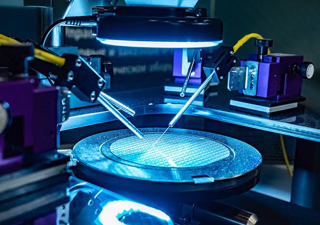
Wafer
Materials & Wafers
The thin, polished disc of single-crystal silicon that chips are built on. The industry standard is 300 mm across and about 775 µm thick.
Wafer bow
WarpMaterials & Wafers
How much a wafer deviates from flat. Stress from deposited films causes it, and too much of it stops lithography focusing correctly.
Wafer map
Metrology, Inspection & Yield
A picture of a wafer showing which dies passed and which failed. The spatial pattern of failures is the first clue to their cause — edge, centre, ring or random.
Wafer probe
Wafer sort, CPTest & Reliability
Electrically testing every die while it is still on the wafer, so bad ones are marked and never packaged. Packaging a known-bad die wastes the most expensive part of the back end.
Warpage
Packaging & ATMP
Bending of a package caused by materials expanding at different rates as temperature changes. Excess warpage breaks solder joints.
Water positive
Sustainability & Energy
Returning or saving more water than the operation consumes, counting replenishment and community projects alongside on-site reclaim.
Water reclaim
Sustainability & Energy
Treating and reusing water already used in the fab rather than discharging it. Leading fabs reclaim well over half of their process water.
Watermark
Cleanroom, Contamination & EHS
A residue stain left when rinse water dries unevenly on a wafer, dissolving a little silicon as it goes. The reason drying method matters as much as rinsing.
Well
n-well / p-wellFront-End Process
A large doped region formed early in the process, inside which transistors of the opposite type are built. CMOS needs both.
Wet bench
Deposition, Etch & Clean
The chemical station where wafers are cleaned or etched in sequenced baths of acids, bases and rinse water.
Wet etch
Deposition, Etch & Clean
Removing material with liquid chemistry. Cheap and highly selective, but it etches sideways as well as down, so it cannot make fine features.
WIP
Work In ProgressSmart Manufacturing & AI
The material currently inside the line. Too little starves tools; too much lengthens cycle time without adding output.
Wire bonding
Packaging & ATMP
Connecting die pads to package pins with hair-thin gold, copper or aluminium wire. Still the highest-volume interconnect method in the industry.
Wire pull
Packaging & ATMP
A destructive test that hooks a bond wire and pulls until something breaks, measuring bond strength and revealing where the weak point is.
WLP
Wafer Level PackagingPackaging & ATMP
Packaging dies while they are still part of the wafer, then dicing. It removes handling steps and produces the smallest packages.
WOW Academy
Industry, Standards & India
WOWSemi's industry-aligned learning and certification arm, organised around the WA-01 to WA-08 skill-domain taxonomy.
WOW Ladder
Industry, Standards & India
WOWSemi's five-rung progression from seeing, to touching, to operating, to being assessed, to being placed — the pedagogy the certification tracks are built on.
WOW NEXT
Wafer On WingsIndustry, Standards & India
WOWSemi's international chapter, taking semiconductor knowledge beyond India's borders. The first corridors are Uzbekistan in Central Asia and Sweden in Northern Europe.
WOWSemi Foundation
Wafer On Wheels Semiconductor FoundationIndustry, Standards & India
An Indian Section 8 non-profit building India's first experiential semiconductor skill development platform, registered in Coimbatore, Tamil Nadu under CIN U85499TZ2026NPL040184.
WOWSemiVerse
Industry, Standards & India
WOWSemi's six connected programmes — Fab On Wheels, WOW Semuseum, WOW Academy, WOW Bot, Semipreneur and Green Fab City — which together run one journey from inspiration to capability.
Wrist strap
Cleanroom, Contamination & EHS
A grounded band worn on the wrist that safely bleeds static charge off a person handling sensitive devices.
WSPM
Wafer Starts Per MonthIndustry, Standards & India
The standard measure of fab capacity, counting how many wafers begin processing each month.
X
X-ray inspection
Packaging & ATMP
Imaging the inside of a finished package with X-rays to see solder joints, wire loops and voids without opening it. The standard non-destructive check on assembly quality.
XRD
X-Ray DiffractionMetrology, Inspection & Yield
Measuring crystal structure, orientation and stress by how a material diffracts X-rays. Used to characterise films and substrates.
XRF
X-Ray FluorescenceMetrology, Inspection & Yield
Measuring the elemental composition and thickness of a film from the characteristic X-rays it emits when excited. Fast, non-destructive and common for metal layers.
Y
Yield
Metrology, Inspection & Yield
The percentage of dies on a wafer that work. Yield decides whether a fab makes money, and hunting the lost percentage is a full engineering discipline.
Z
Zero defect
Industry, Standards & India
The quality philosophy that treats any escape as unacceptable rather than statistically tolerable. Standard expectation in automotive and medical supply.
ZLD
Zero Liquid DischargeSustainability & Energy
Treating wastewater so that essentially nothing is discharged as liquid, with water recovered and solids handled separately. Increasingly a permitting condition in water-stressed regions.

Definitions are written for learners, not for standards committees. Where a term has a formal definition in an ISO, JEDEC or SEMI standard, that standard governs. Spotted something wrong? Tell us at operations@wowsemi.org.

Need help exploring WOWSemi?