 +
+Sivasankari Subburaj
Community & Social Impact
Community-development and social-impact leader — champions skill development and career awareness for students and women across India.
LinkedIn
Founded by community builders. Guided by semiconductor veterans. Built for every student in India.
India was announcing fabs worth billions of dollars while brilliant students a few kilometres away had never seen a wafer.
The talent was everywhere. The exposure was nowhere. So we built a bridge — community leaders on one end, semiconductor veterans on the other.
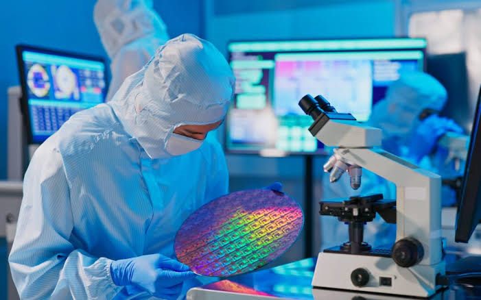
India's first experiential semiconductor skill development platform and ecosystem enabler — where no learner's distance from a fab decides their distance from a semiconductor career.
Take real semiconductor experience to the doorstep of every learner in India — and turn it into skills industry hires for.
WEAVE — Women Empowerment & Advancement by Vision & Excellence. A WOWSemi initiative empowering women through skills, mentorship, leadership and industry access, so they can grow, lead and shape the next generation’s semiconductor future.
+Community-development and social-impact leader — champions skill development and career awareness for students and women across India.
LinkedIn +
+Driven by a passion for training young talent — a creative designer leading AI at WOWSemi and a champion of women in semiconductors.
LinkedIn +
+Profile coming soon.
 +
+Social-work postgraduate (BSW, MSW) leading outreach, educational collaborations and community engagement — connecting students, academia, industry and society.
LinkedIn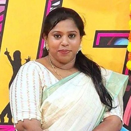 +
+Profile coming soon.
 +
+Profile coming soon.
 +
+Supply-chain and procurement leader with 14+ years across Infosys BPM (Microsoft), Autoliv, Tech Mahindra (Applied Materials), TCS (GE Healthcare) and Flex — supply assurance, demand planning, procurement operations and order management. Lean Six Sigma certified.
LinkedIn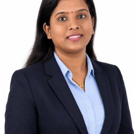 +
+Team Leader at Tech Mahindra — LV electrical systems, control panels and schematics across industrial automation and semiconductor projects.
LinkedInWEAVE is still being written — and there is a place in it for you.
Join WEAVEStrategic leaders — from fab floors, policy rooms, OEMs and campuses — who shape every WOWSemi program. Select any name to read more.
Advisors and mentors serve in a personal capacity. Their employers and institutional affiliations are listed for background only and do not imply endorsement of WOWSemi by those organisations.
 +
+Fab and ATMP/OSAT startup specialist, GM at PTW Semiconductor India — equipment engineering, localization and plant start-up.
LinkedIn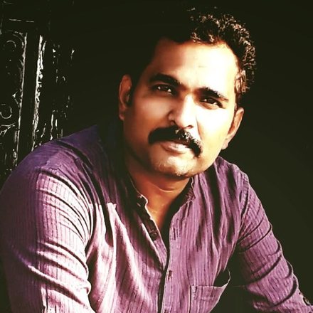 +
+17+ years in semiconductor mechanical design, CAD and technical publication — leads cross-functional design, manufacturing-support and engineering-change teams.
LinkedIn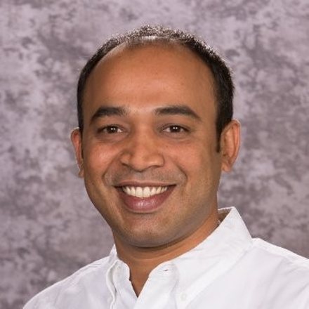 +
+18 years in semiconductor manufacturing across wafer fabs and OSAT — leads ASML EUV equipment operations and operational transformation for high-volume manufacturing.
LinkedIn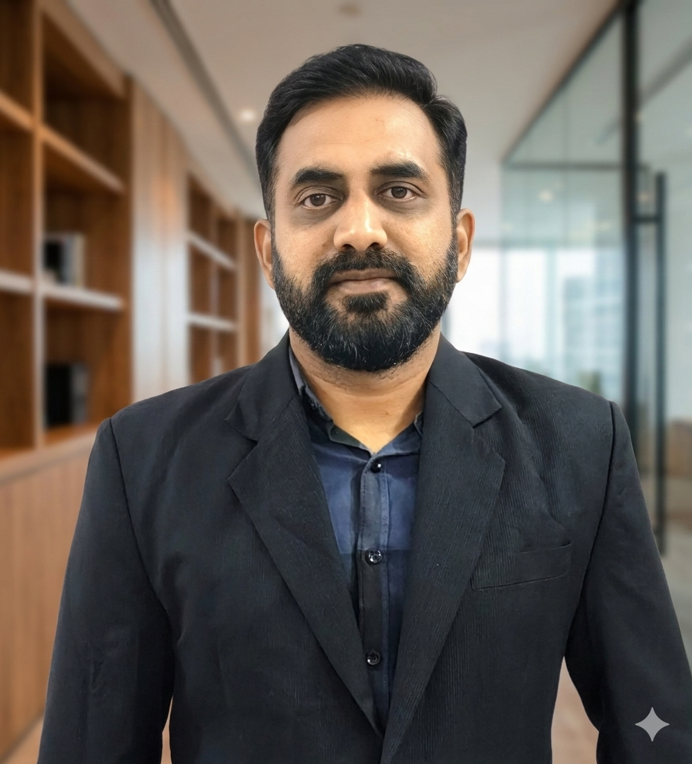 +
+AI innovation and supply-chain strategist across the semiconductor value chain — keeps every WOWSemi program carrying Industry 4.0 DNA, not yesterday's syllabus.
LinkedIn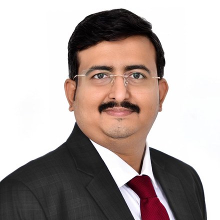 +
+GCC transformation leader with 22+ years across five continents — builds and scales profitable Global Capability Centers in India, the Middle East, UK, Netherlands and Singapore, standing delivery centres up from scratch with governance and internship-to-hire talent pipelines built in. Has worked with EY, Arthur D. Little and Capgemini on national citizen e-services, sovereign cloud and banking programmes. Now focused on AI, semiconductor and quantum computing.
LinkedIn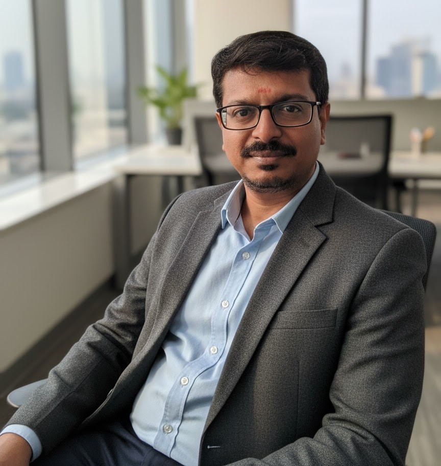 +
+Electronics and Robotics expert and technical-training specialist — shapes the hands-on lab exercises and assessments that turn curious students into job-ready engineers.
LinkedIn +
+Business development and strategic management for cleanroom capital projects in semiconductor and pharmaceutical manufacturing — cross-functional leadership and engineering operations.
LinkedIn +
+Leads Sweden/EU–India flagship programs. European Innovation Council 2026 mentor (Tech to Market · Women Leadership), silicon-carbide platform builder, and a specialist in turning research into real exploitation pathways.
LinkedIn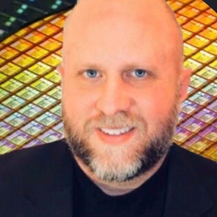 +
+Semiconductor storyteller reaching 12 million industry professionals a year from Austin, Texas. 28 years across Applied Materials, Samsung, Intel, IBM, Texas Instruments and GlobalFoundries — ALD, PVD, EPI and CVD process and field service, then capital-equipment sales, and scaling Moov Technologies from $3M to $50M in revenue.
LinkedIn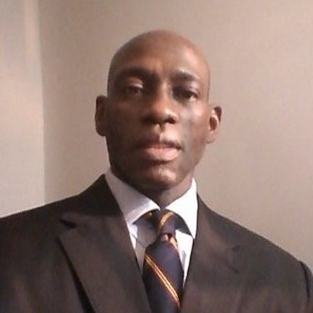 +
+Founder, managing partner and global technology consultant across IT, mobile communications, fintech, blockchain, cybersecurity and AI data-centre infrastructure — a University of California, Berkeley alumnus focused on taking products and services to market.
LinkedIn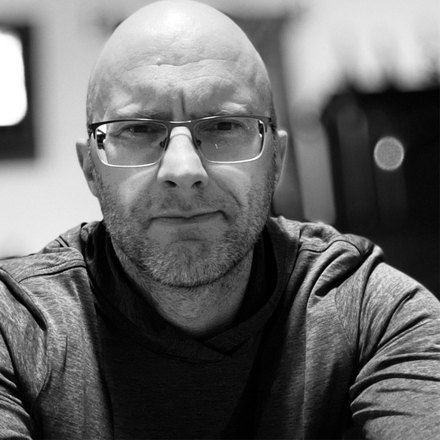 +
+Founder of TechSovereign Partners, working with deep-tech founders and scaling teams to cut through friction and hit critical milestones without slipping into chaos. 27+ years solving make-or-break problems in semiconductor manufacturing and equipment development — process strategy through capital-equipment rollouts. His premise: great technology dies when execution fails.
LinkedIn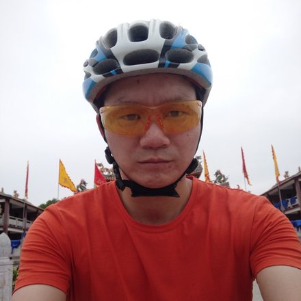 +
+Precision mechanical parts, module machining and semiconductor equipment manufacturing — automated equipment design, tooling and manufacturing solutions for semiconductor, resistor and inductor production, with eight years in automated-equipment mechanical design.
LinkedIn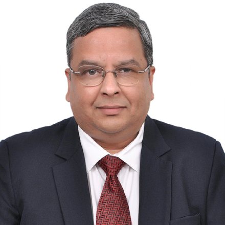 +
+Former President & CEO of IESA and CEO of ESSCI, previously VP at Tata Projects' Advanced Tech Facilities — a leading voice on India's semiconductor policy and fab build-out.
LinkedIn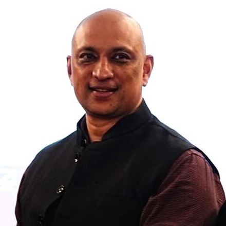 +
+30+ years of senior leadership in strategy, product management and business development at leading global semiconductor and technology companies — startup mentor and angel investor.
LinkedIn +
+Silicon and hardware product development — package design and foundry interface through power-on to PRQ, ATE sort test, characterisation and qualification — across aerospace, semiconductor, telecom and energy.
LinkedIn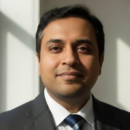 +
+Heads a semiconductor business division — sales, service, manufacturing and new-product development — with a track record of building new business across India.
LinkedIn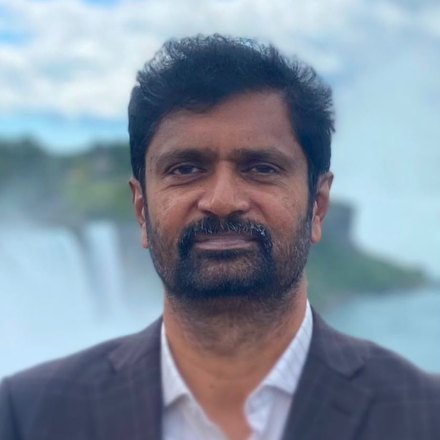 +
+Chief Executive Officer at SHANAN Innovetek Ventures.
LinkedIn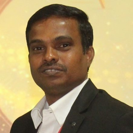 +
+IBU Head and Global Delivery Head at Tech Mahindra — 27+ years leading semiconductor and hi-tech product design, development and delivery worldwide.
LinkedIn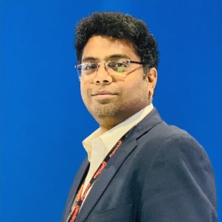 +
+Quality Management System manager — brings fab-grade QMS discipline to WOWSemi's curriculum, safety standards and lab operations.
LinkedIn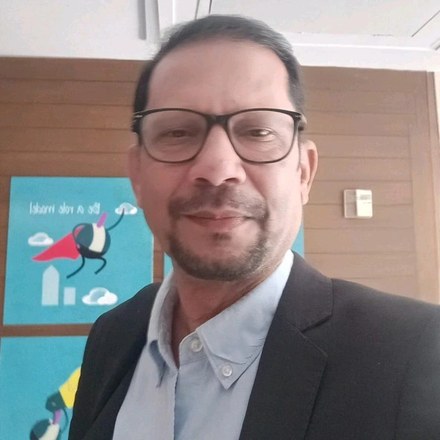 +
+Profile coming soon.
LinkedInIndustry Ideators are practitioners who bring the shop floor into our programs — the people who install the tools, run the projects and supply the lines.
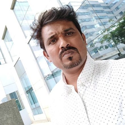 +
+Manager at Siemens Energy with 18+ years across semiconductor engineering, wind and offshore-wind energy — mechanical design, cable and harness systems, project management.
LinkedIn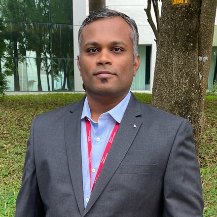 +
+Electrical engineer across semiconductor, display and process industries — control-system design, automated test equipment, testing and commissioning.
LinkedIn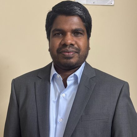 +
+Discipline lead for semiconductor fab design and process engineering — greenfield and brownfield fab projects with EXYTE and GLOBALFOUNDRIES in Singapore.
LinkedIn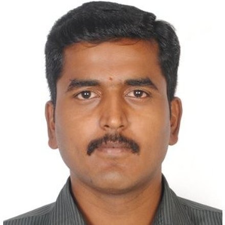 +
+Senior Manager at QUAVAC India.
LinkedIn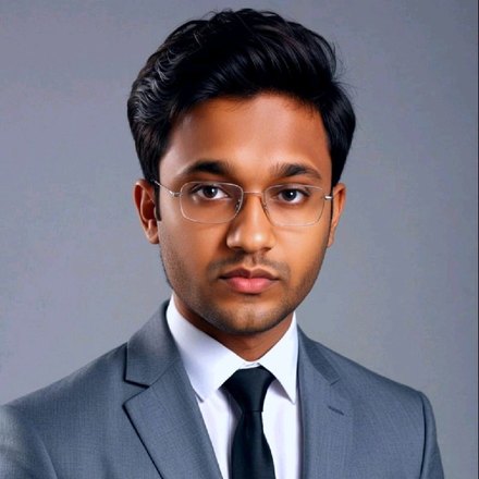 +
+15+ years in digital marketing — digital strategy, programmatic and digital media, advertising operations, account-based marketing, integrated campaigns, SEO, PPC and marketing automation.
LinkedIn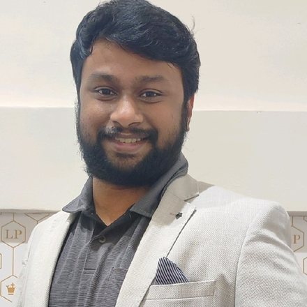 +
+Systems engineering and R&D — previously Applied Materials, Tech Mahindra, SAMEER and Air India — working across automated test equipment, AI/ML, computer vision and robotics.
LinkedIn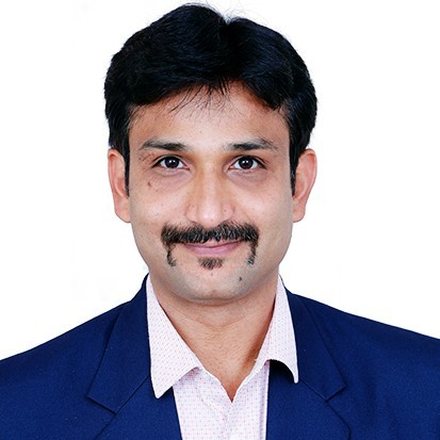 +
+Project manager in the outsourcing and offshoring industry — supports CAD requirements and helps organisations establish extended engineering teams.
LinkedIn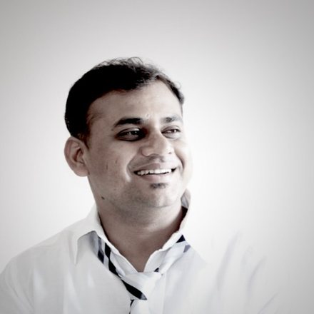 +
+Senior Business Analyst at Applied Materials.
LinkedIn +
+13 years in technology, including 4 in semiconductor tool installation — FI robot setup, load-port integration and tool-server configuration, plus LabWindows/CVI software development, RS232/422 communication protocols and DAQ systems.
LinkedIn +
+Operations and project-delivery leader — formerly Schlumberger across oil, gas and energy, now delivering engineering and production for the bio-pharma industry.
LinkedIn +
+Entrepreneur building in India's emerging semiconductor ecosystem — B2B supply chain for cleanroom consumables such as wipes and gloves, with a long-term vision to scale into manufacturing. Previously a forensic accountant with international exposure in financial analysis, risk and compliance.
LinkedIn +
+14 years across distribution, marketing and manufacturing — now focused on helping shape India's semiconductor industry.
LinkedIn +
+16+ years in RF engineering across telecom — LTE, UMTS and RAN performance and optimization with Huawei, Ericsson and ZTE.
LinkedIn +
+Construction Manager at Best & Crompton Engineering Ghana Limited.
LinkedIn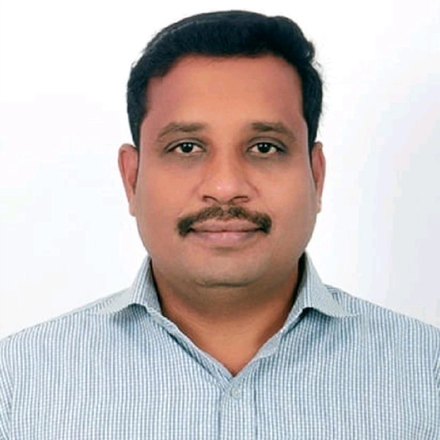 +
+PMP-certified engineering and program-management leader with 21+ years across semiconductor equipment, EPC/MEP infrastructure and industrial R&D — greenfield and brownfield programs, fab tool readiness (FAT, SAT, IQ/OQ/PQ), thin-film deposition tools, utility systems and cleanroom facilities.
LinkedIn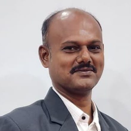 +
+Assistant Professor at SRM Institute of Science and Technology, Ramapuram Campus, Chennai — bridges academic rigour and industry practice for WOWSemi's campus programs.
LinkedInEnabling Ideas. Accelerating Programs. Creating Impact.

Connecting Industry. Creating Access. Evolving the Ecosystem.

The people who carry the mission beyond our own channels — so a learner in a Tier-3 district hears about the bus before it arrives.
Mentor a district. Advise a program. Sponsor a bus. India's semiconductor generation is waiting.