India's first experiential semiconductor skill development platform and ecosystem enabler — real equipment, virtual fabs and AI training, brought to every school and college.
Six ways in. Every one of them puts something real in front of you.
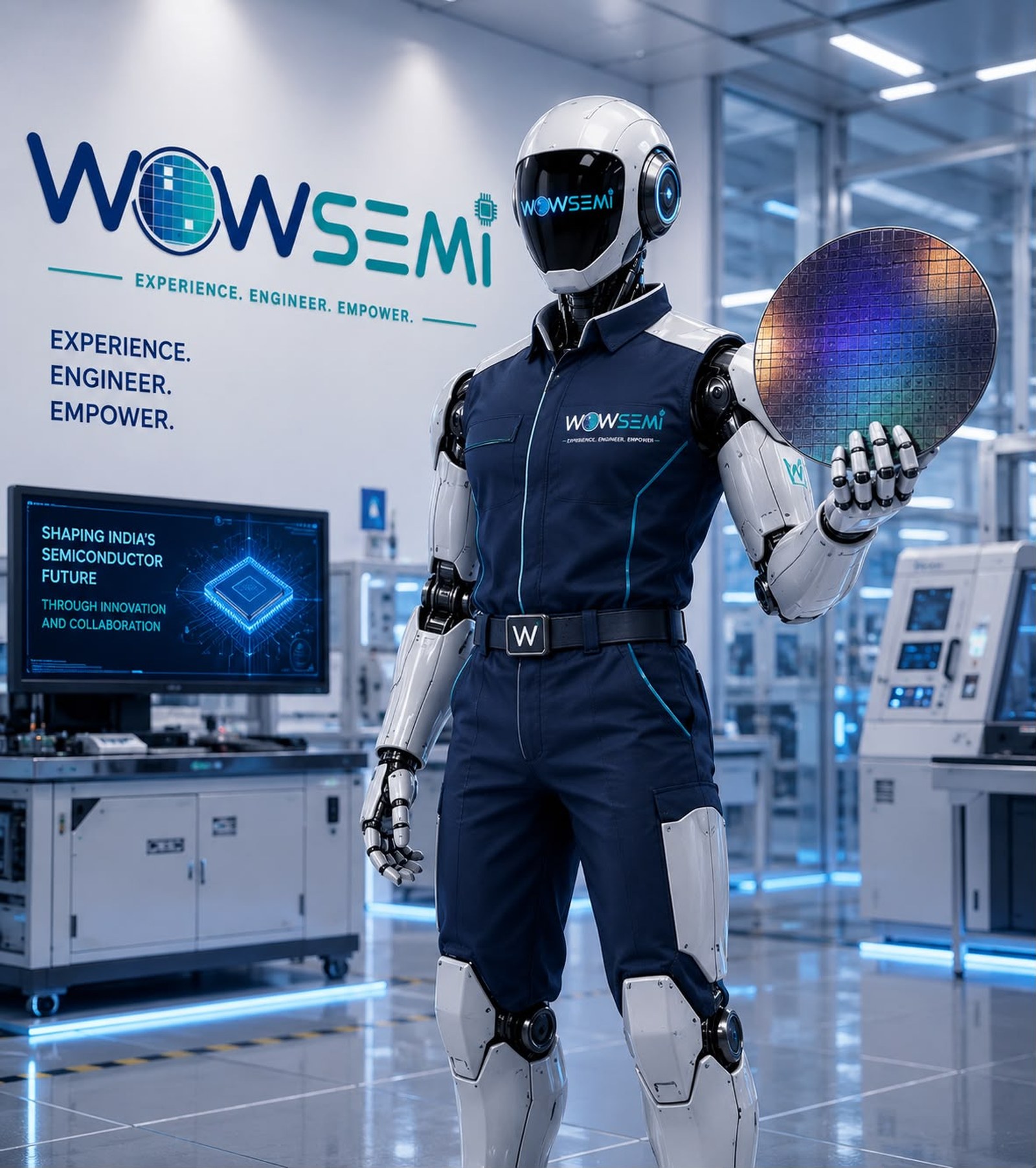
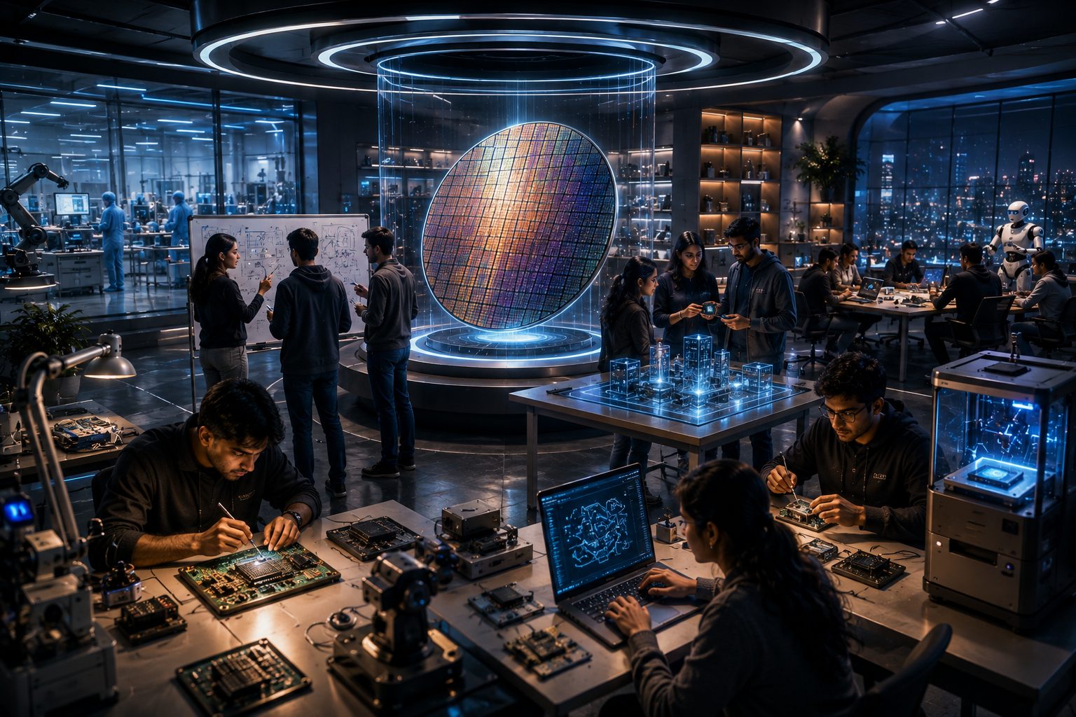
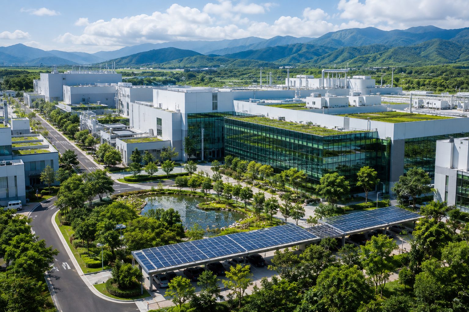
India's fabs are hiring — but most graduates have never touched a wafer. WOWSemi closes that gap with one philosophy: “Experience Before Expertise.”
Not another training organization — a complete semiconductor ecosystem.
Three verbs. One pipeline. First touch to industry-ready.
Touch the real thing — wafers, packages, sensors, equipment.
Run the process — virtual fabs, simulators, failure analysis.
Turn skill into a job — certification, mentoring, placement.
India’s six-pillar semiconductor strategy needs people before it needs anything else. WOWSemi builds Pillar 6 — the manufacturing workforce.
When people are empowered, the entire semiconductor ecosystem grows.
With 315 universities training students on complex chip design using the latest EDA tools, around 68,000 students have already been trained. It will be developed further and deepen the level of training while in college. Further, the industry will be actively engaged in deepening the clean room, fab construction and other ecosystem training as well.Sixth pillar · Semicon India Programme (Semicon 2.0)
Universities are covering chip design. The pillar's second half — cleanroom, fab construction and ecosystem training — needs equipment, not slideware. That is the half WOWSemi builds for, and it is why our bus carries real tools to campuses instead of asking campuses to come to a fab.
One national purpose, delivered through five pillars — with experiential learning, AI, sustainability, women in technology and rural reach woven through all of them.
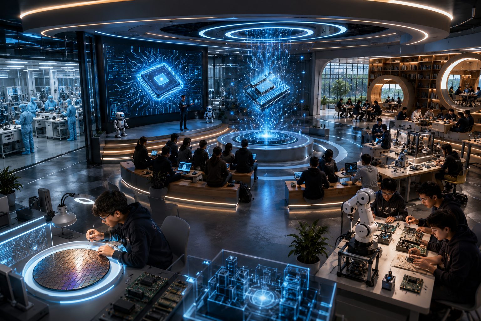
Wafer fab, ATMP/OSAT, equipment engineering, cleanroom and AI — taught hands-on, then certified.
WOW Academy 02Fab On Wheels, mobile cleanrooms and the Semuseum — connecting government, industry, academia and startups.
Fab On Wheels 03Startup incubation, rural STEM, women in semiconductor and youth innovation — inclusive growth, not trickle-down.
Semipreneur 04A transparent, professionally governed Section 8 institution built for long-term public impact.
Trust & Compliance 05Applied research, prototypes, technology transfer and open knowledge — our contribution to Pillar 05.
Research & InnovationSource: the six-pillar strategy announced under the Semicon India Programme. WOWSemi is an independent Section 8 foundation and is not a government body; alignment describes our programme design, not an endorsement.
Progressive, industry-aligned levels. Every course maps to a real fab role and counts toward a WOWSemi certificate.
First cohorts begin 1 December 2026. Levels 01–04 are WOWSemi’s own ladder; every certificate is issued by WOWSemi Foundation. See the certification tracks →
Eighty years of silicon in one scrolling timeline — gold markers are the plot twists.
Bardeen, Brattain & Shockley at Bell Labs replace vacuum tubes with a sliver of germanium. Electronics is reborn.
Jack Kilby demonstrates the first IC at Texas Instruments; Robert Noyce's planar version at Fairchild soon makes it manufacturable.
Gordon Moore predicts transistor counts will double every year — revised to every two years in 1975. The industry turns it into a schedule.
The first commercial microprocessor: 2,300 transistors at 10µm. Your phone now carries billions.
Morris Chang separates design from manufacturing — enabling fabless companies and today's global chip economy.
Design centres bloom in Bengaluru, Hyderabad and Noida — India becomes a global VLSI design powerhouse.
After decades of R&D, ASML's EUV machines — printing with 13.5nm light — enter high-volume chip production.
₹76,000 crore national program launches — India commits to making chips, not just designing them.
Dholera, Sanand, Morigaon — India's first commercial fab and ATMP projects break ground and ramp.
India targets a $100B+ semiconductor economy. The engineers who build it are in classrooms today — WOWSemi is how they get ready.
No one builds a semiconductor workforce alone. The fifth leg — community — is the one most programmes leave out.
Put a WOWSemi lab on the road for a year — your branding on the bus, your engineers as guest mentors, quarterly impact reports on your desk.
Sponsor a bus →Fund awareness drives, faculty training and student workshops across an entire district — measurable, named, and yours.
Adopt a district →Back certification scholarships for talented students and fab-grade lab setups on partner campuses.
Endow a scholarship →Funded through direct grants, philanthropy and co-established CSR programmes. How we structure funding →
Talk to us early and we will work with your compliance team to structure the engagement correctly. Our full registration status →
Community leaders who know how to reach students, and semiconductor veterans who know what fabs actually need — working the same mission.
WOWSemi Foundation is an Indian Section 8 non-profit building India's first experiential semiconductor skill development platform. It takes real wafers, semiconductor equipment and cleanroom discipline directly to schools, ITIs, polytechnics and colleges, so a learner's distance from a fab does not decide their distance from a semiconductor career. It is registered in Coimbatore, Tamil Nadu, under CIN U85499TZ2026NPL040184.
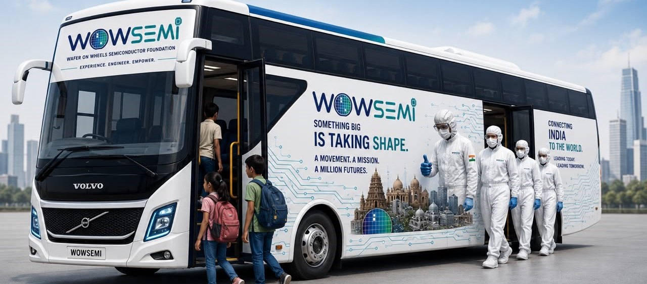
Fab On Wheels is WOWSemi's mobile semiconductor laboratory — a bus carrying real equipment, wafer samples, AR/VR stations and cleanroom protocol training to campuses across India. A single campus day covers cleanroom procedure, wafer and package handling, equipment familiarisation, an electronics bench activity and a careers session.
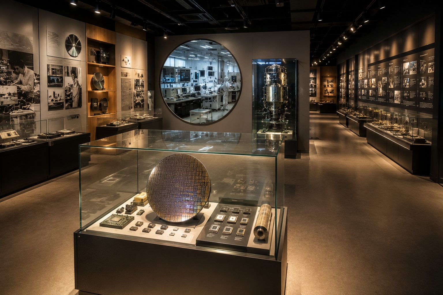
The WOWSemiVerse is WOWSemi's six connected programmes: Fab On Wheels (the mobile lab), WOW Semuseum (a semiconductor knowledge museum), WOW Academy (industry-aligned learning and certification), WOW Bot (a humanoid semiconductor educator), Semipreneur (turning learners into founders) and Green Fab City (sustainable semiconductor manufacturing). Together they run one journey: inspire, experience, learn, interact, innovate, build.
WOWSemi rolls out in four audited phases across eleven states. Phase 1 (2026) covers Tamil Nadu and Karnataka; Phase 2 (2027) Andhra Pradesh and Odisha; Phase 3 (2028) Gujarat, Kerala and Telangana; Phase 4 (2030) Maharashtra, New Delhi, Uttar Pradesh and Assam. Each phase is independently audited before the next opens.
WOW Academy runs 26 certification tracks across eight skill domains coded WA-01 to WA-08: Semiconductor Safety & EHS; Fab & Cleanroom Infrastructure; Equipment Engineering & Automation; Process Engineering & Manufacturing; Facilities, Utilities & Sustainability; Smart Manufacturing & AI; Energy & Resource Management; and Environmental Sustainability & ESG. First cohorts begin 1 December 2026. Certificates are issued by WOWSemi Foundation.
No. WOWSemi Foundation is an independent Section 8 non-profit company registered under the Companies Act, 2013. Its programme design aligns with the Semicon India Programme's sixth pillar — talent development — but that alignment describes WOWSemi's own programme design and is not a government endorsement.
By 2031 WOWSemi targets 5,00,000 citizens reached, 11 states, 60 districts, 3,000 partner institutions, 4 Fab On Wheels buses, 4 Semuseums, 200 startup incubations and 1,00,000 industry-aligned certifications, with 40% women learners and 50% rural participation.
Institutions can host a Fab On Wheels visit or integrate WOW Academy content; companies can donate or loan equipment, fund a bus, adopt a district, endow scholarships or back faculty development through CSR. Every enquiry goes to operations@wowsemi.org.
Whether you're a curious student, a college principal, a fab HR head or a CSR leader — there's a seat on the bus.
HQ · WOWSemi, R-28, C1, D, First Floor, Kovaipudur, Coimbatore - 641042, Tamil Nadu · ☎ +91 90803 25242